We study from fundamental physics to novel electronics
for building modern integrated circuits using atomically thin materials.
Research Interests
The Lan group research focuses on the science and
technology of nanomaterials. Our research is multidisciplinary; the group
includes researchers with diverse backgrounds, including chemistry, physics,
material science, and electrical engineering.
One main research goal is to
study the fundamental physics and build atomically-thin integrated
circuitry. In order to build atomically thin integrated circuitry, we
develop advanced growth, characterization and device fabrication methods for
2D layered materials, which specifically include semiconducting transition
metal dichalcogenides. For the study of fundamental physics, for example, we
reported “Resonant tunneling through discrete quantum states in stacked
atomic-layered MoS2”
(Nano Letters 2014 [6]) and “Strong Rashba-Edelstein Effect-Induced
Spin-Orbit Torques in Monolayer Transition Metal Dichalcogenides/Ferromagnet
Bilayers” (Nano Letters 2016 [2]).
Based on resonant tunneling
phenomenon and other fundamental physics, we would like to extend to another
research goal for exploring novel electrical, optical, piezoelectric,
magnetic and optoelectronic properties of low-dimensional nanostructures.
These will allow the development of advanced devices, including highly
efficient solar cells, ultrasensitive infrared bolometric detectors, and
novel valleytronic and spintronic devices. In the past, we reported "
CVD-grown atomic-monolayer triangular MoS2
piezotronics" (Nature Communications 2015 [5]), “ High-current gain
two-dimensional MoS2-base
hot-electron transistors” (Nano Letters 2015 [4]), “Self-aligned graphene
oxide nanoribbon stack with gradient bandgap for visible-light
photodetection” (Nano Energy 2016 [3]) and “Atomic-Monolayer Two-Dimensional
Lateral Quasi-Heterojunction Bipolar Transistors” (ACS Nano 2017 [1]).
Selected References
1. Che-Yu Lin, Xiaodan Zhu,
Shin-Hung Tsai, Shiao-Po Tsai, Sidong Lei, Yumeng Shi, Lain-Jong Li,
Shyh-Jer Huang, Wen-Fa Wu, Wen-Kuan Yeh, Yan-Kuin Su, Kang L. Wang and
Yann-Wen Lan* “Atomic-Monolayer Two-Dimensional Lateral
Quasi-Heterojunction Bipolar Transistors with Resonant Tunneling Phenomenon”
ACS Nano, DOI: 10.1021/acsnano.7b05012 /
Publication Date (Web): 04 Oct 2017
(Corresponding author*, SCI, impact factor:13.942)
2. Qiming Shao*, Guoqiang Yu*,
Yann-Wen Lan*, Yumeng Shi, Ming-Yang Li, Cheng Zheng, Xiaodan
Zhu, Lain-Jong Li, Pedram Khalili and Kang L. Wang. “Strong Rashba-Edelstein
Effect-Induced Spin-Orbit Torques in Monolayer Transition Metal
Dichalcogenides/Ferromagnet Bilayers” Nano Letters, Accepted in
November, DOI: 10.1021/acs.nanolett.6b03300, 16, 7514-7520, 2016.
(Equal first author*, SCI, impact factor:13.592)
3. Yann-Wen Lan*,
Carlos M. Torres Jr., Xiaodan Zhu, Chia-Liang Sun, Shuanglin Zhu, Chii-Dong
Chen* and Kang L. Wang. “Self-aligned graphene oxide nanoribbon stack
with gradient bandgap for visible-light photodetection. Nano energy,
27, 114-120, 2016. (Corresponding author*, SCI,
impact factor:11.553)
4. Carlos M. Torres Jr.§,
Yann-Wen Lan§,*,
Caifu Zeng, Jyun-Hong Chen, Xufeng Kou, Aryan Navabi, Jianshi Tang, Mohammad
Montazeri, James R. Adleman, Mitchell B. Lerner, Yuan-Liang Zhong, Lain-Jong
Li,
Chii-Dong Chen and Kang L. Wang* “ High-current gain two-dimensional
MoS2-base
hot-electron transistors”. Nano Letters 15, 7905-7912, 2015.
(Equal first author§
and Corresponding author*, SCI, impact factor:13.592)
5. Junjie Qi§,
Yann-Wen Lan§,*,
Adam Stieg, Jyun-Hong Chen, Yuan-Liang Zhong, Lain-Jong Li, Chii-Dong Chen,
Yue Zhang*, and Kang Wang*, "Piezoelectric effect in CVD-grown
atomic-monolayer triangular MoS2
piezotronics" Nature Communications, 6, pp7430, 2015.
(Equal first author§
and Corresponding author*, SCI, impact factor:11.470,
Rank: 3/55)
6. Linh-Nam Nguyen, Yann-Wen Lan*, Jyun-Hong Chen, Yuan-Liang Chung, Kuei-Shu Chang-Liao, Lain-Jong Li, and Chii-Dong Chen*. “Resonant tunneling through discrete quantum states in stacked atomic-layered MoS2” Nano Letters, 14(5), pp 2381-2386, 2014. (Corresponding author, SCI, impact factor:13.592)
Piezoelectric effect in CVD-grown atomic-monolayer triangular MoS2 piezotronics
(Nature communications 6:7430,2015)
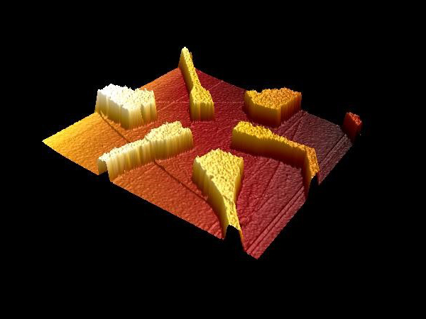
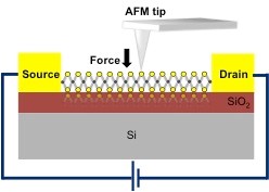
We report the experimental study of the theoretically predicted piezoelectric effect in triangle monolayer MoS2 devices (Figure 1) under isotropic mechanical deformation (Figure 2). The experimental observation indicates that the conductivity of MoS2 devices can be actively modulated by the piezoelectric charge polarization induced built-in electric field under strain variation. These polarization charges alter the Schottky barrier height on both contacts, resulting in a barrier height increase with increasing compressive strain and decrease with increasing tensile strain. The underlying mechanism of strain-induced in-plane charge polarization at zigzag edges is proposed and discussed using energy band diagrams. High-current Gain Two-dimensional MoS2-base Hot-electron Transistors
(Nano Letters 15, 7905–7912, 2015)
We show that by choosing MoS2 and HfO2 for the filter barrier interface and using a non-crystalline semiconductor such as ITO for the collector, we can achieve an unprecedentedly high-current gain (α ~ 0.95) in our hot-electron transistors operating at room temperature. Furthermore, the current gain can be tuned over two orders of magnitude with the collector-base voltage albeit this feature currently presents a drawback in the transistor performance metrics such as poor output resistance and poor intrinsic voltage gain. We anticipate our transistors will pave the way towards the realization of novel flexible 2D material-based high-density, low-energy, and high-frequency hot-carrier electronic applications. Figure 3 (Left) An isometric view of an MoS2-HET device structure. The capital letters E, B, and C represent the emitter, base, and collector, respectively. (Middle) Cross-sectional view of the vertical heterostructure active region with single-layer MoS2 (0.65 nm) as the base. ITO (~45 nm) serves as the collector electrode and an n++ silicon substrate is used as the emitter. A thin SiO2 (~3 nm) tunnel barrier is utilized for hot-electron injection and HfO2 (~55 nm) serves as the filtering barrier. The hot-electrons injected from the emitter (red arrows) are schematically shown. (Right) Energy band diagram depicting the on-state condition. For VCB > 0 (dashed red lines), the hot-electrons tunneling through the emitter-base tunnel barrier have sufficient kinetic energy to overcome the filter barrier and reach the collector.
 Home
Home Members
 Research
 Publications
 Contact
 News/Award
 ASQNL sweet corner

