We study from fundamental physics to novel electronics for building modern
integrated circuits using atomically thin materials.
Research
Interests
The Lan group research focuses on the science and technology of
nanomaterials. Our research is multidisciplinary; the group includes
researchers with diverse backgrounds, including chemistry, physics, material
science, and electrical engineering.
One main research goal is to study the fundamental
physics and build atomically-thin integrated circuitry. In order to build
atomically thin integrated circuitry, we develop advanced growth,
characterization and device fabrication methods for 2D layered materials,
which specifically include semiconducting transition metal dichalcogenides.
For the study of fundamental physics, for example, we reported “Resonant
tunneling through discrete quantum states in stacked atomic-layered MoS2”
(Nano Letters 2014 [6]) and “Strong Rashba-Edelstein Effect-Induced
Spin-Orbit Torques in Monolayer Transition Metal Dichalcogenides/Ferromagnet
Bilayers” (Nano Letters 2016 [2]).
Based on resonant tunneling phenomenon and other fundamental physics, we
would like to extend to another research goal for exploring novel
electrical, optical, piezoelectric, magnetic and optoelectronic properties
of low-dimensional nanostructures. These will allow the development of
advanced devices, including highly efficient solar cells, ultrasensitive
infrared bolometric detectors, and novel valleytronic and spintronic
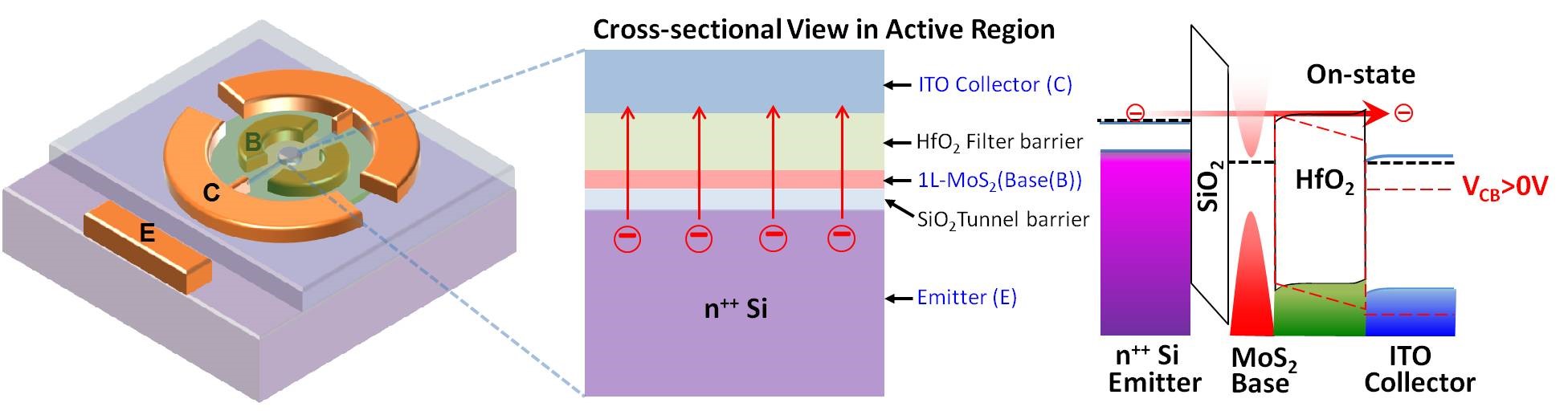
devices. In the past, we reported " CVD-grown atomic-monolayer triangular
MoS2 piezotronics" (Nature Communications 2015 [5]), “
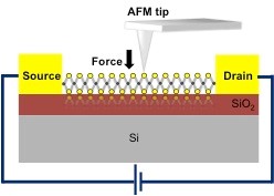
High-current gain two-dimensional MoS2-base hot-electron
transistors” (Nano Letters 2015 [4]), “Self-aligned graphene oxide
nanoribbon stack with gradient bandgap for visible-light photodetection”
(Nano Energy 2016 [3]) and “Atomic-Monolayer Two-Dimensional Lateral
Quasi-Heterojunction Bipolar Transistors” (ACS Nano 2017 [1]).
Selected References
1. Che-Yu Lin, Xiaodan Zhu, Shin-Hung Tsai, Shiao-Po
Tsai, Sidong Lei, Yumeng Shi, Lain-Jong Li, Shyh-Jer Huang, Wen-Fa Wu,
Wen-Kuan Yeh, Yan-Kuin Su, Kang L. Wang and
Yann-Wen Lan* “Atomic-Monolayer
Two-Dimensional Lateral Quasi-Heterojunction Bipolar Transistors with
Resonant Tunneling Phenomenon” ACS
Nano, DOI: 10.1021/acsnano.7b05012
/ Publication Date (Web): 04 Oct 2017
(Corresponding author*, SCI, impact factor:13.942)
2. Qiming Shao*, Guoqiang Yu*,
Yann-Wen Lan*, Yumeng Shi,
Ming-Yang Li, Cheng Zheng, Xiaodan Zhu, Lain-Jong Li, Pedram Khalili and
Kang L. Wang. “Strong Rashba-Edelstein Effect-Induced Spin-Orbit Torques in
Monolayer Transition Metal Dichalcogenides/Ferromagnet Bilayers”
Nano Letters, Accepted in
November, DOI: 10.1021/acs.nanolett.6b03300, 16, 7514-7520, 2016.
(Equal first author*, SCI, impact factor:13.592)
3. Yann-Wen Lan*,
Carlos M. Torres Jr., Xiaodan Zhu, Chia-Liang Sun, Shuanglin Zhu, Chii-Dong
Chen* and Kang L. Wang. “Self-aligned graphene oxide nanoribbon stack
with gradient bandgap for visible-light photodetection.
Nano energy, 27, 114-120, 2016.
(Corresponding author*, SCI, impact factor:11.553)
4. Carlos M. Torres Jr.§,
Yann-Wen Lan§,*,
Caifu Zeng, Jyun-Hong Chen, Xufeng Kou, Aryan Navabi, Jianshi Tang, Mohammad
Montazeri, James R. Adleman, Mitchell B. Lerner, Yuan-Liang Zhong, Lain-Jong
Li, Chii-Dong Chen and Kang L. Wang*
“ High-current gain two-dimensional MoS2-base hot-electron
transistors”. Nano Letters 15, 7905-7912, 2015. (Equal first author§
and Corresponding author*, SCI, impact factor:13.592)
5. Junjie Qi§,
Yann-Wen Lan§,*,
Adam Stieg, Jyun-Hong Chen, Yuan-Liang Zhong, Lain-Jong Li, Chii-Dong Chen,
Yue Zhang*, and Kang Wang*, "Piezoelectric effect in CVD-grown
atomic-monolayer triangular MoS2 piezotronics"
Nature Communications, 6, pp7430,
2015. (Equal
first author§
and Corresponding author*, SCI, impact factor:11.470,
Rank: 3/55)
6.